Fine Focus Scanning Ion Source
- Spot size < 150 µm @ 50 mm working distance.
- Scanning up to 10 mm x 10 mm @ 50 mm
- Keystone correction
- XPS Depth Profiling
- From 5 keV down to 10 eV kinetic energy
- Flux regulation included
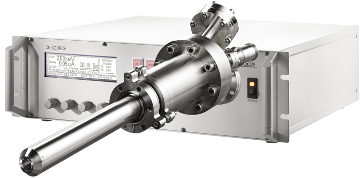
The FDG range of hot filament ion sources, is the premium productline when you need to: clean metals and semiconductors1)-4) or undertake XPS Depth Profiling, ISS/LEIS experiments or as a < 15 eV charge neutralization source. All variants operate as standard with Argon gas but other noble gases or reactive gases like Hydrogen or Oxygen are also fully compatible. Both ion sources are made of completely non-magnetic materials and are compatible with high-resolution electron spectroscopy. An ultra clean ion beam is ensured by an indirect filament, a direct gas inlet for minimizing dead volume and effective differential pumping.
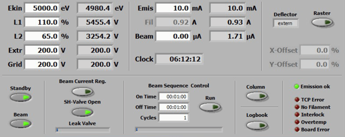
The power supply can be fully controlled with the front panel or via a TCP/IP interface. ProIon, an easy to use LabVIEWTM – based PC software is provided.
Technical Details
The dedicated ion optics allows focusing the spot size down to < 150 µm @ 50 mm working distance. Alternatively a broad spot profile can be chosen for homogeneous large area sputtering.
The integrated raster generator allows for key-stone corrected scanning which in combination with the small spot size and high ion beam currents makes the FDG 150 the ideal tool for XPS and Auger depth profiling with a very homogeneous ablation rate.
In addition, the source comes with a high stability emission current based flux regulation.
The source can be operated with or without differential pumping. The latter provides improved residual gas pressure of typ. 10-8 mbar.
The integrated low energy mode provides a comparable large ion current below 500 eV.
Ion sputtering of semiconductors at low energies (< 100 eV) close to the threshold energy is critical to minimise ion implantation and surface damage1)-4).
Lower energy ion sputtering, at 50 eV, even maintains the sample magnetisation during XPS depth profiling5) and for < 10 eV the source becomes an effective tool for charge neutralization in ESCA applications.
Minimum Spot Size
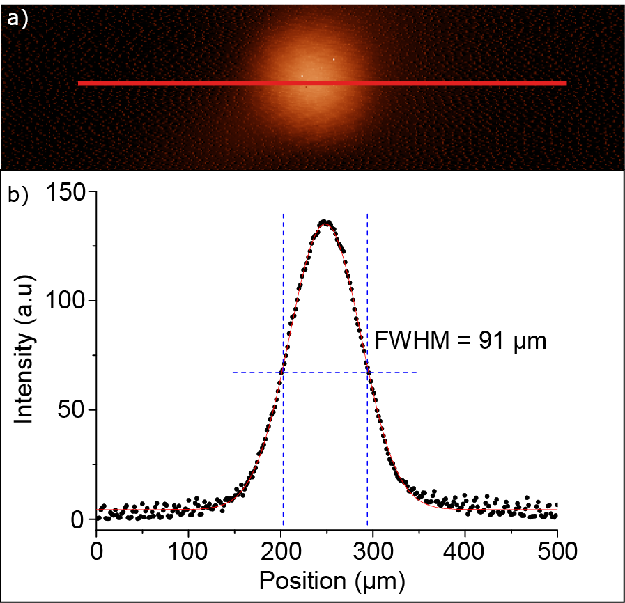
a) Image of the argon ion spot scanned across a 50 µm aperture.
b) Cross section along the red line of a) showing a minimum spotsize @ 5 keV and 1.6 µA.
Apt. corrected real width: (76.4±0.4)µm
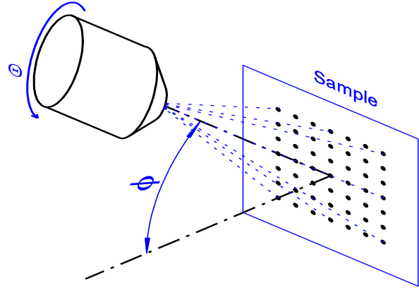
Illustration of Keystone Correction
In order to achieve a homogeneous sputter rate across the sputtered sample area, any tilt φ or rotation θ, between ion source and sample, can be compensated to maintain an undistorted raster field.
XPS depth profiling
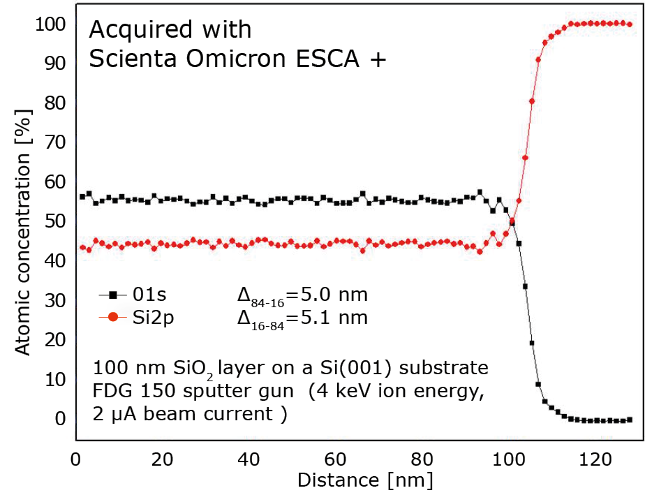
XPS depth profiling through a 100 nm SiO2 layer on Si (001): The cross-over position of the Oxygen peak (O1s) and Silicon peak (Si2p) intensities indicates the thickness of the oxide layer. The FDG 150’s small spot size of 150 µm and the Keystone correction are essential to achieve high precision in depth resolution. To shorten measurement time, both features allow to adjust the sputter area with the energy analyser’s field of view as well as the x-ray source spot size.
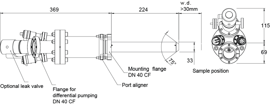
Technical Drawing
Specifications
The table shows the FDG 150 specifications in comparison to the FDG 15.
| Features | FDG 15 & power supply | FDG 150 & power supply |
|---|---|---|
| Mounting flange | DN 40 CF | DN 40 CF |
| Working Distance (WD) | 30 to 300 mm | 30 to 300 mm |
| Min. beam diameter (D) | < 300 μm (@ 5 keV and 50 mm WD) | < 150 μm (@ 5 keV and 50 mm WD) |
| Beam energy 1 | 500 eV to 5 keV> 15 μA (@ 5 keV and 50 mm WD) | 500 eV to 5 keV> 15 μA (@ 5 keV and 50 mm WD) |
| Beam energy 2 | optional | 10 eV to 500 eV; > 1 µA @ 50 eV |
| Beam current density | > 4 mA/cm2 with > 5 µA, D < 350 µm (@ 5 keV and 50 mm WD) | > 4 mA/cm2 with > 5 µA, D < 200 µm (@ 5 keV and 50 mm WD) |
| Scan area | not available | up to 10 mm x 10 mm (@ 5 keV and 50 mm WD) |
| Beam current regulation | ✓ | ✓ |
| Integrated Port Aligner | ✓ | ✓ |
| Current measurement | ✓ | ✓ |
| TCP/IP Interface | ✓ | ✓ |
| LabVIEW based software | ✓ | ✓ |
| Fully non-magnetic | ✓ | ✓ |
| Yttria coated tungsten filament (compatible with O2) | ✓ | ✓ |
| Tungsten filament (compatible with H2) | optional | optional |
| Leak Valve | optional | optional |
1) Chebotarev, S. N. et al. “Low-Energy Ion Technique for Semiconductor Surface Preparation.”
Solid State Phenomena, doi:10.4028/www.scientific.net/ssp.284.198;
2) Dongwan Seo et. al. „Behavior of GaSb (100) and InSb (100) surfaces in the presence of H2O2 in acidic and basic cleaning solutions”, doi.org/10.1016/j.apsusc.2016.12.114
3) Shiou-Min Wu et al. “Sputtering yields of Ru, Mo, and Si under low energy Ar+ bombardment”, Journal of Applied Physics 106, 054902 (2009); doi: 10.1063/1.3149777
4) Hye Chung Shin et al. “Sputter damage in Si surface by low energy Ar+ ion bombardment”, Current Applied Physics 3 (2003) 61–64
5) B. J. McMorran et al., Measuring the effects of low energy ion milling on the magnetization of Co/ Pd multilayers using scanning electron microscopy with polarization analysis. Appl. Phys. 107, 09D305 (2010);
https://doi.org/10.1063/1.3358218